PCB Layout
PCB Layout:
1.1 Introduction:
PCB layout is a necessary part of electronics development. While breadboards and perfboards are fine for prototyping, fabrication and manufacturing for a production run require a fully functional and professional circuit board. There are several options regarding circuit design tools, but we will focus on three common ones: Eagle, KiCAD and Altium. While there are substantial differences between these programs, there are also many topics and practices that are ubiquitous across platforms.
1.2 Key Terms:
Trace/Track - the wires that connect components on a circuit board
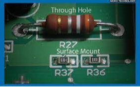
Traces connecting through-hole components on a PCB
Via - holes of various sizes that connect layers on a circuit board
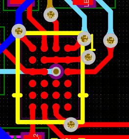
Vias are shown with net and layer labels
Polygon/Pour - an area of various shape and size made of copper, usually used as a ground plane
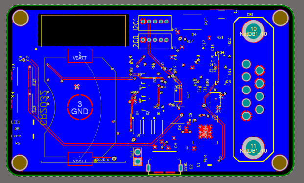
The above image shows a bottom layer polygon pour that serves as the ground plane
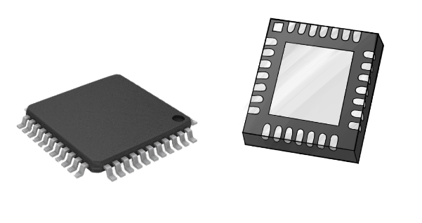
IC - integrated circuit, or a chip
Through-hole - components whose legs go all the way through the pcb and are typically soldered by hand. This is as opposed to
Surface-mount - components that are soldered to the top (or bottom) of the circuit board and do not traverse any layers.
Layer - These make up the PCB “stack”. PCBs can be 1 to almost 100 layers, but are typically 2 to 8, in multiples of 2. A 2-layer board will have tracks and polygons on the top and bottom layers.
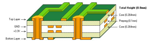
The typical layers are:
Substrate Layer - The substrate layer of any PCB is usually made from fiberglass, which gives the board its rigid form. Generally speaking, the majority of boards will have this material for their substrate, with the exception of flexible PCBs, which are built on flexible plastic such as Kapton. Substrate PCB layers can also be made with other materials such as epoxies, however they lack the durability that FR4 (found in fiberglass) provides for a high quality board.
Copper Layer - Next is a thin layer of copper foil which is laminated to the board using heat. When we are speaking of different layered PCBs, we are referring to how many copper layers they consist of. If you are creating a single-sided PCB the circuit board has one layer of conducting material on one side of the board and the other side is used for incorporating different electronic components. Whereas double-sided PCBs can mount the conductive copper and components on both sides of the board, as opposed to just the one. These double-sided boards allow for closer routing traces as they can alternate between the top and bottom layers using vias. This can be very useful in many electronic products as the circuits on one side of the board can be connected to the other with the help of holes drilled into it.
The thickness of the copper layer on your PCB will depend on the power the PCB needs to withstand. PCBs that need to handle very high power throughout may have a thicker copper layer than those that do not.
Soldermask layer - Once the copper layer has been applied the soldermask layer is placed on top. This gives the PCB its green color and is used to insulate the copper layer to avoid any contact with any other metal or elements of the board that could disrupt the copper traces. This layer is also important for themanufacturing processwhere the components are soldered onto the board, as it helps the user to solder to the correct places.
Silkscreen layer - The silkscreen is mainly for the purpose of us humans to help us better understand the board and the functionality of different pins or LEDs, by adding letters, numbers and symbols to the board.
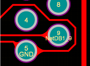
Net - a collection of pads and tracks that are all connected. No two different nets can be connected.
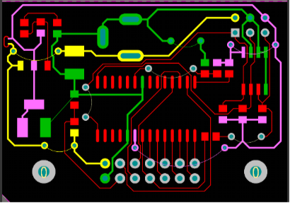
Here every color represents a different net