Slip Ring Project
About the Project
We will be creating a pcb slip ring that lights up 2 LED lights with a USB C Connector!
Slip rings are devices that allow electrical contacts through rotating bodies.
Usually you would simply buy a slip ring, so the question remains, why reinvent the slip ring if it already exists?
My excuse was that they're expensive. Most especially ones with a through hole in the center :(
Slip rings are a good way to practice PCB and CAD design. And they kinda cool too!!
Challenges
Kicad
We will be making this with KiCAD, a PCB making software. This will be a good intermediate level KiCAD tutorial. Later we will be ordering and assembling our PCB with some SMD components.

CAD
Very minimal CAD in this lesson. There are only 2 parts that will be needed to be designed.
Code
No Code.
Materials
PCB Making
- Mouser account
- JLCPCB Account
- 5mm breadboard LEDs
- Solder Paste
Mechanical
- Snap ring pliers
- Retaining Rings
- 1/4" Ball Bearing
- M4 Grub Screws
- 1/4" Shaft
- Assorted M3 Bolts
The Plan
Use USB-C (because it is the future) as a power-input device to power on an LED. This LED will be able to spin indefinitely and still be powered on because it will be on a slip-ring.
There will be two boards that we make:
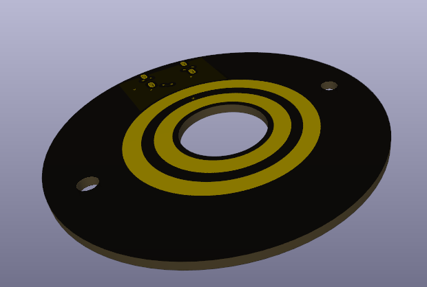
Ring side
- USB C Female end
- Current limiting resistor for the LEDs
- CC Resistors
- Shell Resistor
- Exposed copper rings
- Two mounting holes
- One large through hole straight through the center
Contact side
- Female dupont pins for the 5mm LEDs
- Spring contacts that will establish an electrical connection with the other pcb
Power through USB C
To get 5V from USB C, it is not as simple as just using the VCC lines. Although just using the VCC line for Type A -> USB C cables, this does not work for USB C -> USB C cables or "smart" USB C power supplies.
USB C needs a way to acknowledge what type of device is downstream and what voltage to supply at what current. This is where the CC data lines off of the USB C port come in to play. 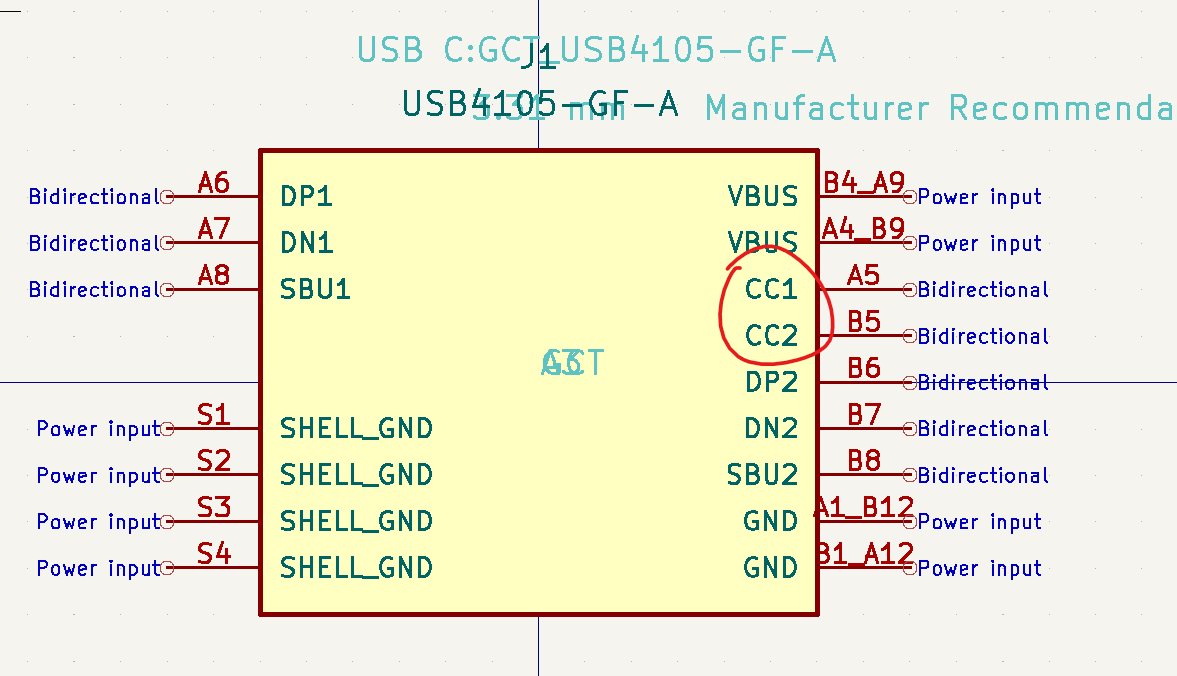
In order to "tell" our power supply what voltage / current we need. Simply connect two 5.1kΩ pulldown resistors to both CC1 and CC2.
You'll also notice that there is a SHELL_GND. These are the legs connected to the USB C port. Instead of wiring these directly to GND, they should go through a resistor so that there isn't a ginormous short in the case of a loose power wire. Since we are already using 5.1kΩ resistors, we'll just use a resistor to limit the current.
Setting up KiCAD
Create a new project in KiCAD. You can name it "Baby slip ring"
Importing Components
Because at the time I am writing this, this USB C is in stock and super cheap. Therefore we will be using this one. Unfortunately, not everything that you want to use will already be pre-imported into KiCAD for you. Therefore you must be familiar with importing things (unless you want to make everything yourself).
Downloading Files
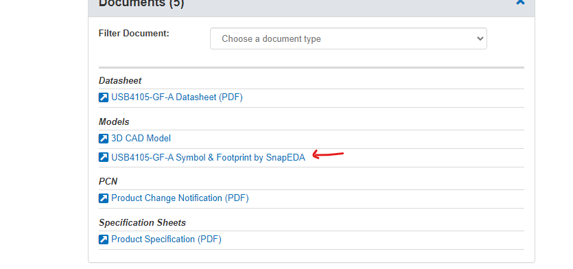
To import this you want to scroll down to where it says you can find the Models and click on the link to SnapEDA.
- I like SnapEDA because they are very consistent with providing good quality symbols, footprints, and models.
- I like SnapEDA because they are very consistent with providing good quality symbols, footprints, and models.
Click on Download symbol and footprint
Select KiCAD 6.0
Unzip the installed folder and place it inside of your project folder
Importing Footprints
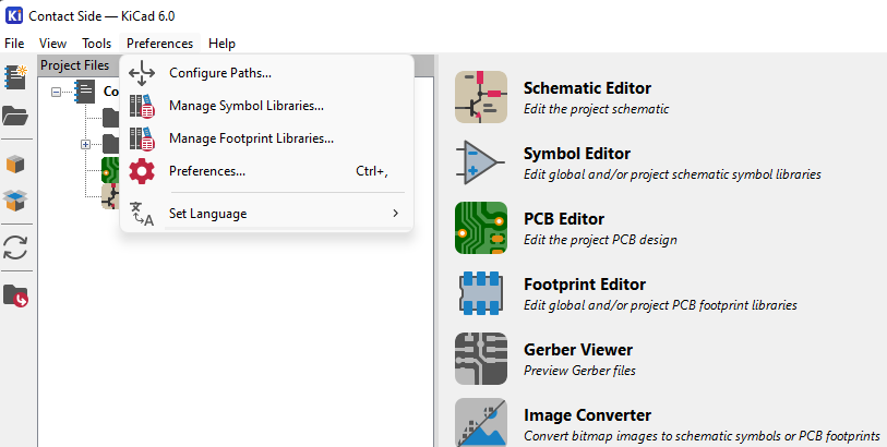
- Click on Manage footprint libraries under the Preferences menu of KiCAD's main menu
- Click on the Project specific libraries tab at the top of your screen
- Click on the plus button in the bottom left hand corner of the window.
- Name the new entry a good description like "USB C" and then link the correct Path to the library by clicking on the Folder icon
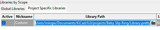
- Now click on "Migrate libraries" in the bottom right corner of the screen and click "OK"
- Open the imported footprint in the Footprint Editor to verify that it was successfully imported
Importing Schematics
- Click on Manage symbol libraries under the Preferences menu of KiCAD's main menu
- Click on the Project specific libraries tab at the top of your screen
- Hit plus button in bottom left corner
- Name the new entry (Purple circle)
- Click on the library logo and select the path to the USB C's .lib file
- Click Migrate Libraries in the bottom right hand corner of your screen
- Press OK
- Now open the file in the symbol editor and verify that it is correct
- Press E whilst still in the symbol editor to open the properties menu
- Change the footprint path to be updated and correct by clicking on the little 3 vertical bars menu under "Footprint"
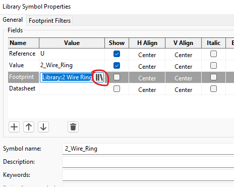
- Under the Datasheet entry, copy/paste in the link to the product page.
Using KiCAD
Making the Ring Side
Rings
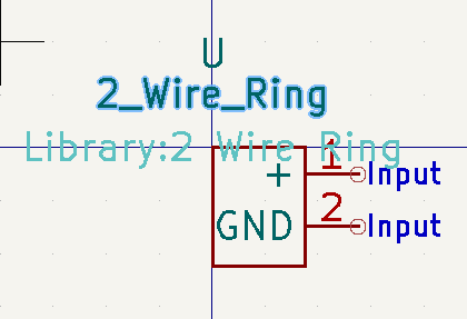
First we are going to want to make a 2 pin symbol for the Rings.
- Open up the symbol editor and create a new symbol, simply titled "2 Wire Ring"
- Draw a simple box with 2 pins. One will be power and the other will be ground Power will have a designator of one and GND will have designator 2.
Next we should make the footprint for our symbol.
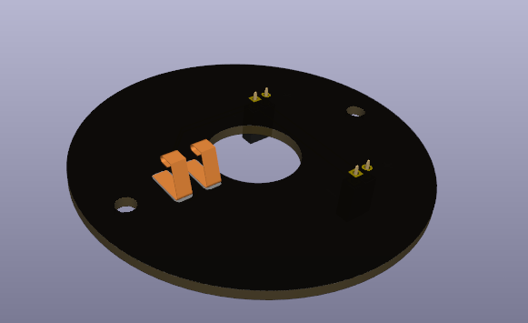
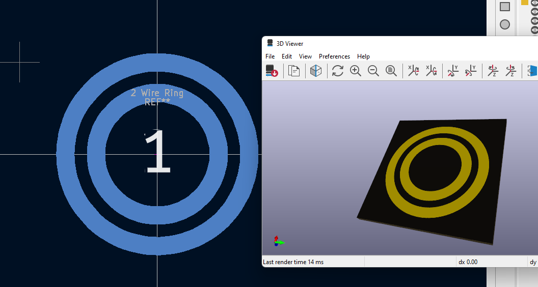
The end result should look something like the image below
- Open up the footprint editor
- Make a circular pad that is 10.16mm from the origin. The pad must should be 3mm in diameter with no through hole
- Now right click on the pad and click on "Edit pad as graphical shape" (Ctrl+E) is the shortcut.
- While in this menu, any shape you draw will be a pad. Make a circular ring with the center point at the origin and the end point on the circle. Change it's thickness to be 3MM
- Repeat the steps except with a ring that is 15.24mm from the center and having designator of 2.
- Now click on both of the rings and press "F" on your keyboard. This switches it to the bottom copper layer
- Readjust the rings so that they are centered on the footprint editor again, if neccessary
- Ensure that your footprint looks something like this:
Now go back to your 2 wire ring symbol and press "E" to edit the properties. Link the footprint to the one that you just made in the last step.
Finding the 5.1kΩ resistors
We will need to find exactly what resistors we are going to buy since we are going to use Power through USB C
- Go to Mouser
- Navigate to Passive components -> Resistors -> SMD Resistors/Chip Resistors
- Now use the filters to find the correct resistor that we want.
- Criterias:
- Panasonic (since they're a good brand)
- 5.1kΩ
- 0402 or 0603 size
- Hit "Apply Filters" when done
- Now click on the first part that comes up and that is in stock. Save the link to the product page for later.
Finding the 470Ω resistors
Follow the directions for the Finding the 5 1kΩ resistors except do it for 470Ω resistors. This is our current limiting resistor for the 5mm LED
change it to be more simple
Making the Schematic
Ensure that you have properly installed the symbol and footprint library for our USB C
- Open the project schematic
- Drag in the USB C, 2 Wire Ring, and 2 generic Resistor symbol
- Click on one of the Resistors and press "E" to edit it's properties.
- Change the value to 5.1k
- Change the footprint to a SMD Resistor either 0402 or 0603 in size (whatever you chose)
- Paste in the link to the product page for the Datasheet row
- Do the same for the other Resistor, except it is the 470Ω variant
- Copy/Paste in two more 5.1k resistors.
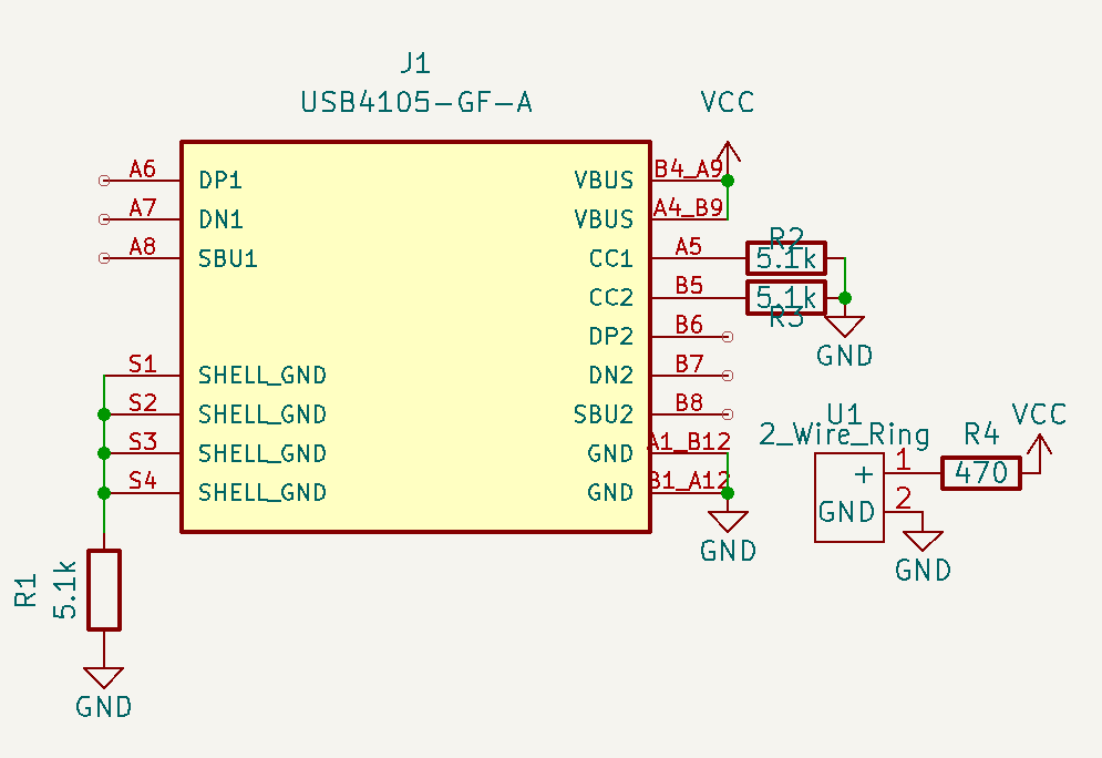
- Follow the schematic below
Making the PCB
Press "U" on keyboard to import everything into a PCB. Annotate the board if not already done so.
- Make two cocentric circles on the edge cuts layer to define our board outline. One should be 7.64mm in radius and the other 28.74mm in radius.
- Ensured that the Rings are cocentric with the board outline.
- Make USB C Port stick out directly to the right of the center of the circle (orange arrow) . I would reccomend overhanging the USB C port off the edge of the board (red arrow) a bit to ensure that a cable would be able to plug into it.
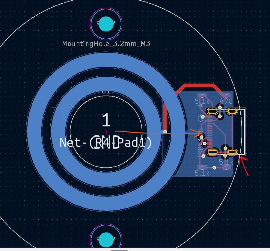
- Click on the "Add a footprint" button and find the "MountingHole_3mm".
- Place two mounting holes directly above and directly below the center of the slip ring. Each hole should be 22.86mm from the center of the ring.
- Place the passive components closely around the USB C port.
- Route all the traces.
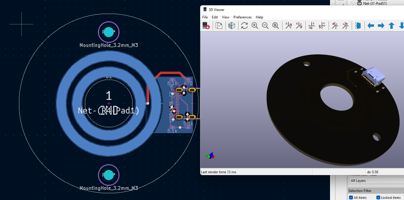
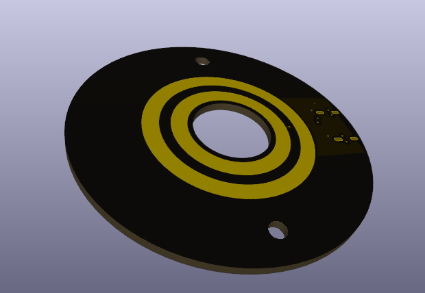
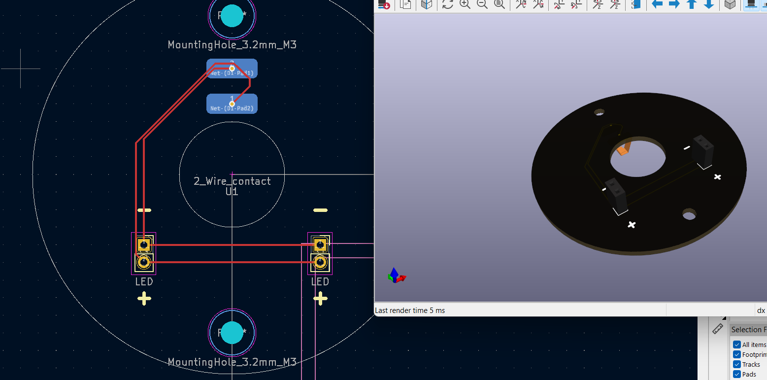
- Press Alt+3 and verify that it looks something like this:
Making the Contact Side
Create a new project titled "Contact Side"
SMD Contact Footprint
We will be using these spring contacts. The datasheet says that they are rated for sliding and have a height of 5.7mm. Both of which are important for the mechanical aspect of this slip ring.
Now we will be making the footprint to hold these contacts.
- Click on the above link to the spring contacts and open the datasheet.
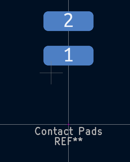
- Create a new footprint within the Contact Side project
- Follow the "RECOMMENDED PCB LAYOUT" to create two rectangular pads.
- Press "F" on both of your pads to move them to the bottom copper layer.
- One of them should be 10.16mm (designator 1) and the other 15.24mm (designator 2) from the center
Create a copy of the 2 Wire Ring symbol that you made in the previous step. Except that this one will be for the 2 Spring Contacts.
Now go back to your newly copied smybol and press "E" to edit the properties. Link the footprint to the one that you just made in the last step.
Making the Schematic
- Create a new schematic
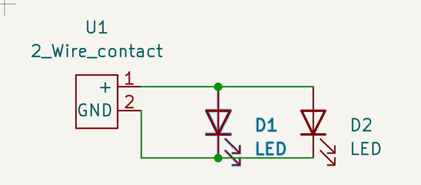
- Draw in the 2 Spring Contact symbol that you made in the previous step
- Also import in two generic LEDs.
- Edit the properties of both of the LEDs
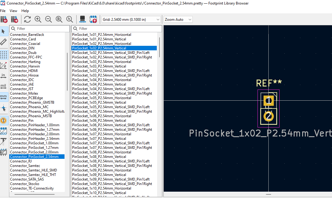
- Set the footprint of the LEDs to simply just be a 1x2 dupont pin
- Connect your schematic's traces like so
Making the PCB
- Copy up to step 1 in the previous section's Making the PCB
- Ensure that the origin of your Spring contacts are cocentric with the board outline.
- Again, click on the "Add a footprint" button and find the "MountingHole_3mm". Place two mounting holes directly above and directly below the center of the slip ring. Each hole should be 22.86mm from the center of the ring.
- Put the LED Duponts 12.7mm to the right of the origin and 10.16mm down
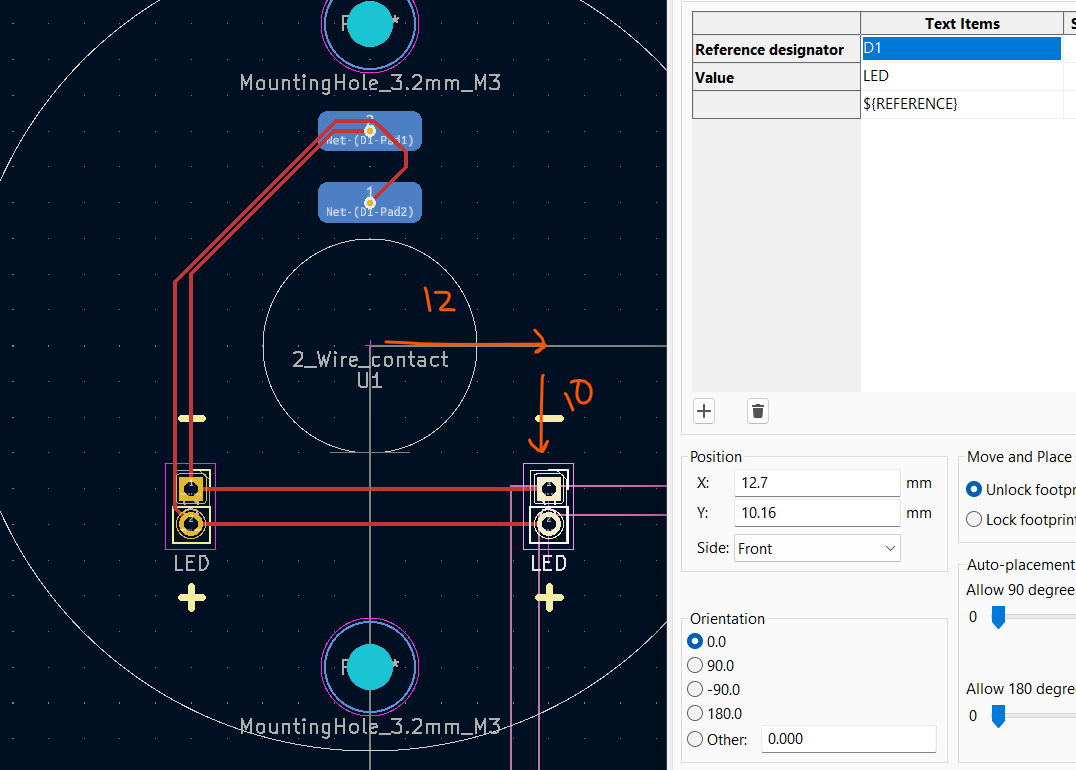
- Complete the same but mirrored about the y axis
- Wire up the PCB
- Add text on the Front Silkscreen layer indicating the positive and negative end of the LED
Ordering
This is the final step. Make sure that you have made these PCBs correctly and ran the DRC check or else when these pcb's come and they're incorrect it willl be a sad day.
Exporting machining files for JLCPCB
- With the PCB open, press Plot (Printer icon in top left)
- Under output directory create a new folder in the project folder named "exports" (this will make exporting easier). Then select that folder you just created as your output directory.
- Generate drill files (bottom right). Then hit the Generate drill file again on the window that just pops up
- Close and hit "Plot"
- Now compress to zip file on the exports folder
- Now do the same but for the other PCB
Ordering from JLC's Website
- Go to JLCPCB
- Upload the Ring side zip file to JLCPCB
- Select the PCB color that you want (Black is usually the best color)
- Because this has small SMD components that you aren't going to be able to solder by hand, we are going to need to order the stencil.
- Scroll down to the bottom of the order page and enable the stencil option
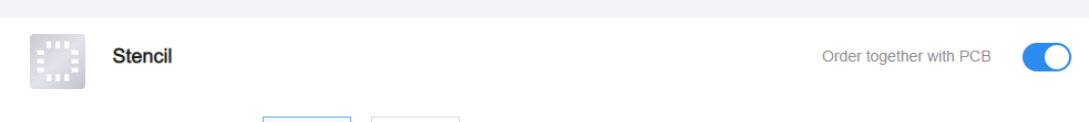
- Repeat the same step except for the Contact side zip file. Know that you do not need to order the stencil as well with the Contact side board.
Ordering from Mouser
Now we need to order our electrical components from Mouser. As a good rule of thumb, I always order double the quantity of any passive component I may need. Reasoning being that if you fuck up or drop them, they are so small that they are probably gone forever.
Remember that you can simply click on the link that you assigned to each component under the "Datasheet" column.
Order list:
- 2x USB Cs
- 6x 5.1kΩ Resistors
- 2x 470Ω Resistors
- 4x SMD Spring Contacts
Ordering from Amazon
Make sure that you have all the mechanical components that is required to assemble the PCB, since the actual PCB takes about 1-2 weeks to arrive.
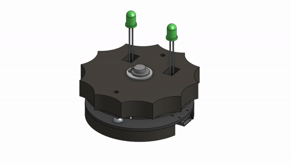
3D Printing
Print out the required files for the assembly of the actual slip ring. (Power Input and Output side parts)
Assembly
USB C Side
Watch from 2:15 - 3:53 of this video The video demonstrates the technique that we'll be using for the side of the PCB with a USB C connector .
- We will stick our desired PCB to the table with some tape
- We can lay some of our extra pcbs around to make it an even surface for us to place our stencil on
- We align our stencil so that it matches with the pads on our pcb
- Stick it down with tape
- Spread out the paste
- Carefully put on the components with really fine tweezers
- Now instead of using a hot air gun like in Great Scott's video, we will simply be using the PCB at Envision to melt our PCBs
Contact Side
- Hand solder the spring contacts onto the board. It doesn't matter which way they are facing
- Solder female header pins on the opposite side of where the spring contacts are
Final assembly
You can now refer to the CAD Model to complete the final assembly with all the fasteners and 3D printed parts.
- Attach each ring to its respective 3D printed mount with M3 bolts
- Insert 1/4" flanged bearings into the top and bottom hole of the spring contact side
- Insert a relatively short 1/4" axle into the bearings
- Add Snap rings on either side
- Thread on the grub screw into the hole on the ring side
- Insert shaft from the Spring contact side into the hole for in the ring side
- Adjust amount of contact to be just the right amount of rub without too much noise
- Tighten the grub screw, locking the shaft when satisifed
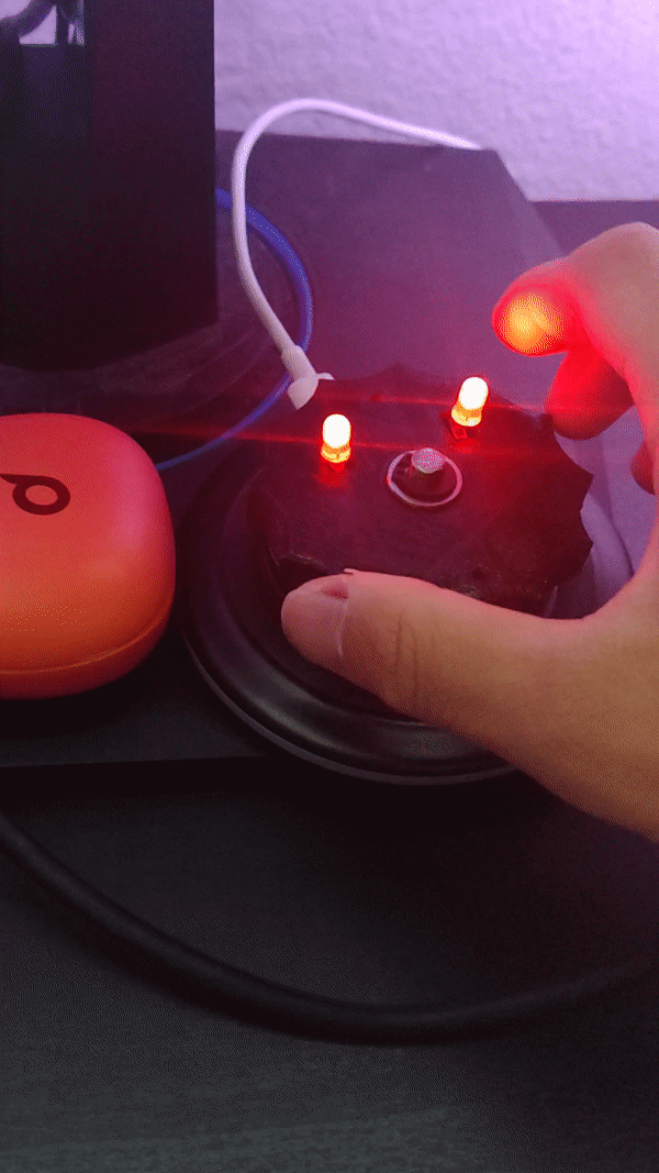
- Insert 5mm LEDs, making sure to get the polarity correct
- Plug it in and watch it spin!